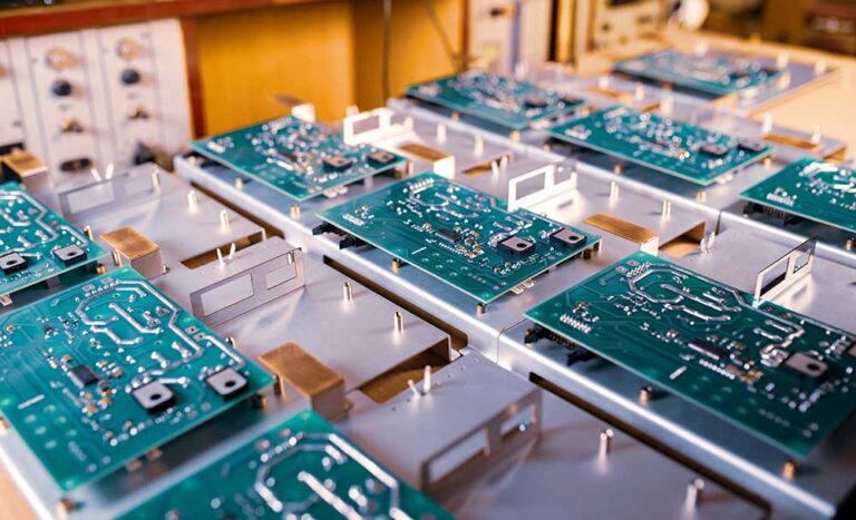
With the advancement of technology, multi-layer printed circuit boards (PCBs) have become commonplace in electronic devices. These multi-layer PCBs offer significant benefits to device manufacturers, such as increased performance and reliability due to their more complex circuitry.
However, many are unaware of the unique manufacturing process associated with these components. In this article, we will delve into the world of multi-layer PCBs and explore the benefits they present for device manufacturers as well as understanding how they are manufactured.
Well also discuss some best practices when using them in your designs so you can get the most out of your electronics projects.
Benefits of Using Multi-Layer PCBs
Multilayer PCB techology provides a variety of benefits, including increased density and reliability. Due to their multiple layers, they can be used for more complex applications than single-layer boards, such as increasing the number of electrical components that can fit on one board or creating a smaller footprint.
This in turn makes multilayer PCBs ideal for products where space and weight are at a premium. Furthermore, with each layer having its ground plane and power planes it offers greater shielding from electromagnetic interference (EMI) compared to other types of boards. In addition, these boards have improved thermal capabilities which is beneficial in high-powered applications; plus the use of blind vias enables access to both sides of the board without compromising circuit integrity.
As if those weren’t enough advantages already, manufacturing costs are also reduced due to their ability to be produced using automated processes rather than manual labor as traditional designs requires. All this adds up to why multi-layer PCBs should be seriously considered when designing your next product!
Manufacturing Challenges of Multi-Layer PCBs

Manufacturing multi-layer PCBs can be a complex undertaking due to the multiple layers of different materials that come together in one board. The process requires precision and accuracy, as any mistakes could end up being costly or even dangerous.
Manufacturers need to take into account all aspects of the product design before production begins, such as its size, number of pins, thickness, and material type. Careful attention must also be paid throughout the entire manufacturing process – from assembly through testing – to ensure quality control and safety standards are met. Additionally, it is important that each layer within the PCB line up perfectly with one another during fabrication; this ensures optimal performance of the device without compromising on quality or functionality.
Conclusion
In conclusion, Multi-layer PCBs offer a multitude of advantages compared to their single-layer counterparts. With the ability to reduce size, weight, and complexity while improving reliability and signal integrity, they are an ideal choice for many applications.
Furthermore, advances in manufacturing technology have made multi-layer PCBs easier and faster to produce than ever before. As such, their use is only likely to continue growing in importance as more applications call for higher-performance circuit boards.
